
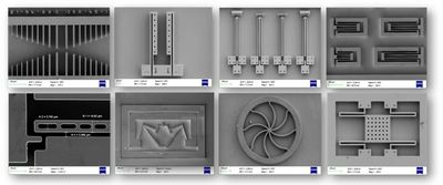
MEMS Devices Fabrication using SOI Process
Users are requested to submit their design layout in the prescribed area of 11 mm x 11 mm out of which 9 mm is the usable design area as per the design rules recommended by INFAB. Upon design submission, 16 chips, will be delivered in 8-10 weeks.
The motivation is to benefit MEMS users at large by providing these devices at affordable cost with less turn-around time. In addition, INFAB is willing to provide support to the users on three crucial aspects: Fabrication cost, turnaround time & Technical support at various stages.
The services are not just limited to microfabrication but also to help the users with technical support such as design feasibility, characterization, packaging, etc. Besides, INFAB also helps with intellectual property such as patents, considering the user’s interest.


Multi Project Wafer MEMS
We offer a Silicon-On-Insulator-Multi-User MEMS Process (SOI) for the fabrication
MEMS device designs from multiple users are shared on a single SOI wafer or a single chip of 1 cm2 in size
LAYER PROPERTIES
The overall process consists of microfabrication of MEMS devices on a SOI wafer using three masks levels that are PAD METAL, SOI, and TRENCH, respectively. METAL layer for the contact; SOI layer for devices; and TRECNCH for back-side etching, are being used in this technology.
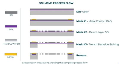
DEVICE LAYER PROPERTIES
Single-Crystal-Silicon (SCS) is used as a structural layer. SOI wafer of three different thickness (10 µm, 20 µm, and 30 µm) as a device layer are used in this process. The Resistivity (ohm-cm) of the device layer (Si) will be in range of 1 - 20 ohm-cm (in bulk), depending upon thickness. User can request for thickness as per their device and design requirement.
Microfluidics Fabrication
The INFAB Polymer-based Microfluidics platform enables the development of Microchannel, Reservoirs, and Microreactors.
PDMS-based Device (Thickness: ranging from 100um to 5mm & widths from 5µm to 250µm
SU8-based Devices (Thickness: from 5µm to 100µm & Width 5µmto 250µm)
